


 Global Sourcing Spotlight: Golf, Friedman, and the Benefits of Global Sourcing
 Nolan’s Notes: Coming to Terms With AI
 The Knowledge Base: A CM’s Perspective on Box Build Practices
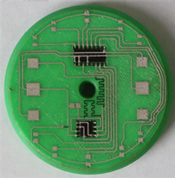
Advanced Printing for Microelectronic Packaging
March 11, 2015 | Kenneth H. Church, Xudong Chen, Joshua M. Goldfarb, Casey W. Perkowski, Samuel LeBlanc, nScrypt Inc.Estimated reading time: 16 minutes
Electronic packaging has been a stable research topic since the vacuum tube era. These were physically large and fragile devices and typically the electronic connection was a mechanical socket that ensured good contact over a large surface area. The issues involved were both electrical contact and mechanical security or ruggedness. The evolution of electronics from vacuum tubes to semiconductors presented opportunities to shrink the electronic devices without reducing the performance. This dramatic change forced a change in connections as well and the idea of mechanically connecting electronics needed to be studied. Solder was a very old, literally thousands of years old [1], technology, but for electronics was a natural fit. A natural fit given two reasons, one was the obvious electrical attributes, but the second was the mechanical flex that solder could provide between two joining surfaces [2]. This became especially important with two dissimilar surfaces. Solder also became its own research topic and the growth and maturity of this process has proven to be one of the most important contributions to electronic packaging since the semiconductor; almost all electronic devices today have solder. The mechanical bond was important, but this alone was not enough given the rugged requirements of some of the electronic devices. The extra ruggedness would be provided using mechanical devices and if the electronics were too small, then another technology that was also thousands of years old was used, glue [3]. Adhesives primary contribution was to enhance ruggedness but adding features such as conductivity to adhesives provided additional value. Solders and adhesives are an important part of electronic packaging and the future of electronics is to increase functions per volume which implies tighter pitch and smaller traces, smaller pads, smaller solder dots and finer features in adhesive patterns. This requires improved methods for applying solder and adhesives. This paper will cover in part, advanced dispensing of fine resolution solder and adhesive dots and lines.
Additionally, just as electronic packaging has evolved from mechanical connections to solder, a future of monolithic electronic packaging will evolve. The idea of circuits in structures has been presented previously by Church et el [4]. Additional demonstrations of printed circuit structures will be shown and the concept of using similar technology to dispensing dots and lines of solder and adhesive will be explained. The concept of dispensing a wide range of materials in three dimensions presents a potential change in electronic packaging. This paper will cover the concept of combining dispensing technologies on a single platform to build integrated and monolithic electronic structural circuits.
Micro-dispensing
There are a number of technologies that can be utilized for micro-dispensing. The technology utilized for the results in this paper is from the standard company micro-dispenser. This has two distinct characteristics that have proven a significant advantage for dispensing very small volumes of solder and adhesive. The first is the specialty shaped pen tip that allows extremely high viscosities (greater than 10 Mcp) and the second is the valve in proximity to the pen tip for exceptional control. Very small volumes such as single digit nanoliter or even less than nanoliter volumes are dimensions of interest with respect to dot size. 300 micron pads are of interest for solder, but the future of solder pads will be much small than 300 microns; 100 microns and less. A 100 micron solder dot will be a need in the near future and it is even conceivable to move toward 50 micron solder dots. A 300 micron solder dot will have a volume of approximately 8 nanoliters (assuming a half sphere shape). An 80 micron solder dot will have a volume of approximately 130 picoliters, a fraction of a nanoliter.
Figure 1 below is a table showing ½ sphere shaped contours diameter versus volume. Controlling small volumes in a
repeatable manner will be important when considering small volumes.
Figure 1. Half sphere diameters converted to volumes.
In addition to dots, there is the need to print fine lines of adhesives or conductive adhesives and other materials. Adhesives can vary significantly in material attributes. These attributes are such properties as viscosity, thixotropy and particle loading. The ability to print adhesive materials consistently and also handle the wide range of diverse properties from the vast array of available materials can be important. The contribution this team has made is to do that with exceptional control for small volumes, provide finer features of 150 microns or less and to control the starts and stops of the dispensed lines and features.Page 1 of 3
Share on:


Suggested Items
Indium Experts to Present at Electronics in Harsh Environments SMTA Conference
05/13/2024 | Indium Corporationndium Corporation Technical Manager for Europe, Africa, and the Middle East, Karthik Vijay, will deliver a technical presentation and Indium Corporation Senior Technologist, Dr. Ronald Lasky, will deliver both a workshop and technical presentation at the Electronics in Harsh Environments SMTA Conference on May 14-16 in Copenhagen, Denmark.
Connect the Dots: Designing for Reality—The Pre-Manufacturing Process
05/08/2024 | Matt Stevenson -- Column: Connect the DotsI have been working with Nolan Johnson on a podcast series about designing PCBs for the reality of manufacturing. By sharing lessons learned over a long career in the PCB industry, we hope to shorten learning curves and help designers produce better boards with less hassle and rework. Episode 2 deals with the electronic pre-manufacturing process. Moving from CAD (computer-aided design) to CAM (computer-aided manufacturing) is a key step in PCB manufacturing. CAM turns digital designs into instructions that machines can use to actually build the PCB.
AIM Solder Signs Shinil Fl Ltd. as New Distributor for Korea
05/08/2024 | AIM SolderAIM Solder, a leading global manufacturer of solder assembly materials for the electronics industry, is pleased to announce a new distribution partnership with Shinil Fl Ltd., a prominent supplier of technological solutions in the SMT and semiconductor sectors.
Indium Corporation to Showcase HIA Materials at ECTC
05/07/2024 | Indium CorporationAs an industry leader in innovative materials solutions for semiconductor packaging and assembly, Indium Corporation® will feature its advanced products designed to meet the evolving challenges of heterogeneous integration and assembly (HIA) and fine-pitch system-in-package (SiP) applications at the 74th Electronic Components and Technology Conference (ECTC), May 28‒31, in Denver, Colorado.
Indium Corporation Expert to Present on Pb-Free Solder for Die-Attach in Discrete Power Applications
04/30/2024 | Indium CorporationIndium Corporation Product Manager – Semiconductor Dean Payne will present at the Advanced Packaging for Power Electronics conference, hosted by IMAPS, held May 8-9 in Woburn, Massachusetts, USA.