


 The Chemical Connection: Reducing Etch System Water Usage, Part 2
 It’s Only Common Sense: Nice Guys Really Can Finish First
 The Right Approach: I Hear the Train A Comin'
Ansys Joins TSMC's OIP Cloud Alliance for Secure Multiphysics Analysis in the Cloud
April 27, 2023 | ANSYSEstimated reading time: 1 minute
Ansys announced that it has joined TSMC's OIP Cloud Alliance to facilitate the deployment of fully distributed workflows for mutual customers. By driving toward the cloud interoperability of Ansys multiphysics solutions with TSMC's technology enablement, customers will easily be able to gain the full benefits of faster run times and elastic computing with major cloud vendors.
Combining EDA parallelism and cloud scalability, TSMC and its OIP Cloud Alliance partners are creating next-generation, cloud-optimized design methodologies to further accelerate turnaround time of critical design tasks. Ansys and other EDA partners will optimize their tools for multi-threaded, fully-distributed runs to best utilize cloud, while cloud partners will bring new virtual machines most suitable for the EDA workload of IC designs.
"Our customers of all sizes are leveraging the cloud to boost productivity while designing in TSMC's leading-edge technologies for new applications from high performance computing to mobile, artificial intelligence, networking, and 3D-IC," said Dan Kochpatcharin, head of the Design Infrastructure Management Division at TSMC. "By welcoming Ansys as the latest member into our OIP Cloud Alliance, TSMC aims to make Ansys' leading multiphysics signoff solutions available to all of our customers and help them bring their differentiated products to market sooner, with higher quality."
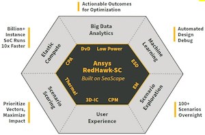
Ansys was an early adopter of elastic cloud computing with its SeaScape big-data platform – a cloud-native data infrastructure that was designed specifically for EDA. Ansys® RedHawk-SC™ was the first tool built to work with SeaScape (SC) and many other Ansys semiconductor tools have followed, including Ansys® PathFinder-SC™, Ansys® Totem-SC™, and Ansys® PowerArtist-SC™.
"Ansys' strategy for the future foresees an absolutely central role for cloud computing," said John Lee, vice president and general manager of the semiconductor, electronics, and optics business unit at Ansys. "We have invested heavily in cloud-enabled platforms that give our products clear advantages in speed and capacity over traditional tool environments that were not designed for the cloud."
Share on:


Suggested Items
Real Time with… IPC APEX EXPO 2024: My Role as a Technology Solutions Director
05/02/2024 | Real Time with...IPC APEX EXPOPeter Tranitz, senior director of technology solutions at IPC, shares insights into his role as the design initiative lead. He details his advocacy work, industry support, and the responsibilities of the design initiative committee. The conversation also covers the revamping of standards, the IPC Design Competition, and the implementation of design rules in software tools.
Real Time with… IPC APEX EXPO 2024: Ventec Discusses New Pro-bond Family of Advanced Products
05/01/2024 | Real Time with...IPC APEX EXPOChris Hanson, Ventec's Global Head of IMS Technology, outlines the launch of four pro-bond formulas that deliver an outstanding combination of low dissipation factor (Df) with a dielectric constant (Dk) range to maximize the design window for critical PCB parameters. As Chris points out, Pro-bond is designed for low-loss, high-speed applications, while thermal-bond dissipates heat from a component through the board to a heat sink.
IPC's Vision for Empowering PCB Design Engineers
04/30/2024 | Robert Erickson, IPCAs architects of innovation, printed circuit board designers are tasked with translating increasingly complex concepts into tangible designs that power our modern world. IPC provides the necessary community, standards framework, and education to prepare these pioneers as they explore the boundaries of what’s possible, equipping engineers with the knowledge, skills, and resources required to thrive in an increasingly dynamic field.
On the Line With… Talks With Cadence Expert on SI/PI for PCB Designers
05/02/2024 | I-Connect007In “PCB 3.0: A New Design Methodology—SI/PI for PCB Designers,” subject matter expert Brad Griffin, Cadence Design Systems, discusses how an intelligent system design methodology can move some signal and power integrity decision-making into the physical design space, offering real-time feedback.
iNEMI Packaging Tech Topic Series: Role of EDA in Advanced Semiconductor Packaging
04/26/2024 | iNEMIAdvanced semiconductor packaging with heterogenous integration has made on-package integration of multiple chips a crucial part of finding alternatives to transistor scaling. Historically, EDA tools for front-end and back-end design have evolved separately; however, design complexity and the increased number of die-to-die or die-to-substrate interconnections has led to the need for EDA tools that can support integration of overall design planning, implementation, and system analysis in a single cockpit.