


 The Right Approach: I Hear the Train A Comin'
 It’s Only Common Sense: OCCAM—the Time Is Now
 Marcy's Musings: The Growing Industry
NIST, Google to Create New Supply of Chips for Researchers and Tech Startups
September 15, 2022 | NISTEstimated reading time: 2 minutes
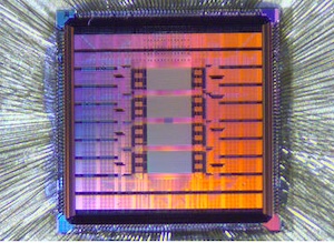
The U.S. Department of Commerce’s National Institute of Standards and Technology (NIST) has signed a cooperative research and development agreement with Google to develop and produce chips that researchers can use to develop new nanotechnology and semiconductor devices.
The chips will be manufactured by SkyWater Technology at its Bloomington, Minnesota, semiconductor foundry. Google will pay the initial cost of setting up production and will subsidize the first production run. NIST, with university research partners, will design the circuitry for the chips. The circuit designs will be open source, allowing academic and small business researchers to use the chips without restriction or licensing fees.
Large companies that design and manufacture semiconductors often have ready access to these types of chips. But the cost can run into the hundreds of thousands of dollars, presenting a major hurdle to innovation by university and startup researchers. By increasing production to achieve economies of scale and by implementing a legal framework that eliminates licensing fees, the collaboration is expected to bring the cost of these chips down dramatically.
“By creating a new and affordable domestic supply of chips for research and development, this collaboration aims to unleash the innovative potential of researchers and startups across the nation,” said Under Secretary of Commerce for Standards and Technology and NIST Director Laurie E. Locascio. This collaboration was planned before the recent passage of the CHIPS Act, but, Locascio said, “This is a great example of how government, industry and academic researchers can work together to enhance U.S. leadership in this critically important industry.”
Modern microelectronic devices are made of components that are stacked like layers in a cake, with the bottom layer being a semiconductor chip. The NIST/Google collaboration will make available a bottom-layer chip with specialized structures for measuring and testing the performance of the components placed on top of it, including new kinds of memory devices, nanosensors, bioelectronics and advanced devices needed for artificial intelligence and quantum computing.
NIST anticipates designing as many as 40 different chips optimized for different applications. Because the chip designs will be open source, researchers will be able to pursue new ideas without restriction and share data and device designs freely.
“This is a great example of how government, industry and academic researchers can work together to enhance U.S. leadership in this critically important industry.” —Under Secretary of Commerce for Standards and Technology and NIST Director Laurie E. Locascio
"Google has a long history of leadership in open-source,” said Will Grannis, CEO of Google Public Sector. “Moving to an open-source framework fosters reproducibility, which helps researchers from public and private institutions iterate on each other’s work. It also democratizes innovation in nanotechnology and semiconductor research.”
The SkyWater foundry will produce the chips in the form of 200-millimeter discs of patterned silicon, called wafers, which universities and other purchasers can dice into thousands of individual chips at their own processing facilities.
The 200mm wafer is an industry standard format compatible with the manufacturing robots at most semiconductor foundries. Giving researchers access to chips in this format will allow them to prototype designs and emerging technologies that, if successful, can be integrated into production more quickly, thus speeding the transfer of technology from lab to market.
Research partners contributing to the chip designs include the University of Michigan, the University of Maryland, George Washington University, Brown University and Carnegie Mellon University.
Share on:


Suggested Items
Koh Young Showcases Award-winning Inspection Solutions at SMTconnect with SmartRep in Hall 4A.225
04/25/2024 | Koh Young TechnologyKoh Young Technology, the industry leader in True 3D measurement-based inspection solutions, will showcase an array of award-winning inspection and measurement solutions at SMTconnect alongside its sales partner, SmartRep, in booth 4A.225 at NürnbergMesse from June 11-13, 2023. The following offers a glimpse into what Koh Young will present at the tradeshow:
Real Time with… IPC APEX EXPO 2024: Plasmatreat: Innovative Surface Preparation Solutions
04/25/2024 | Real Time with...IPC APEX EXPOIn this interview, Editor Nolan Johnson speaks with Hardev Grewal, CEO and president of Plasmatreat, a developer of atmospheric plasma solutions. Plasmatreat uses clean compressed air and electricity to create plasma, offering environmentally friendly methods for surface preparation. Their technology measures plasma density for process optimization and can remove organic micro-contamination. Nolan and Hardev also discuss REDOX-Tool, a new technology for removing metal oxides.
Nanotechnology Market to Surpass $53.51 Billion by 2031
04/25/2024 | PRNewswireSkyQuest projects that the nanotechnology market will attain a value of USD 53.51 billion by 2031, with a CAGR of 36.4% over the forecast period (2024-2031).
Cadence, TSMC Collaborate on Wide-Ranging Innovations to Transform System and Semiconductor Design
04/25/2024 | Cadence Design SystemsCadence Design Systems, Inc. and TSMC have extended their longstanding collaboration by announcing a broad range of innovative technology advancements to accelerate design, including developments ranging from 3D-IC and advanced process nodes to design IP and photonics.
SMC Korea 2024 to Highlight Semiconductor Materials Trends and Innovations on Industry’s Path to $1 Trillion
04/24/2024 | SEMIWith Korea a major consumer of semiconductor materials and advanced materials a key driver of innovation on the industry’s path to $1 trillion, industry leaders and experts will gather at SMC (Strategic Materials Conference) Korea 2024 on May 29 at the Suwon Convention Center in Gyeonggi-do, South Korea to provide insights into the latest materials developments and trends. Registration is open.