


 The Right Approach: I Hear the Train A Comin'
 It’s Only Common Sense: OCCAM—the Time Is Now
 Marcy's Musings: The Growing Industry
New SIA Map Highlights Broad U.S. Semiconductor Ecosystem
March 29, 2023 | SIAEstimated reading time: 1 minute
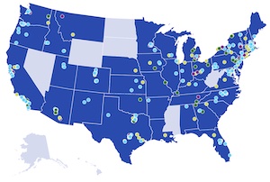
The semiconductor ecosystem in the United States is broad and diverse, as illustrated by SIA’s new U.S. Semiconductor Ecosystem Map, a first-of-its-kind tool that allows users to explore industry activities across the country, including nearly 500 locations in 42 states. This expansive ecosystem is comprised of semiconductor manufacturing, chip design, intellectual property and chip design software providers, semiconductor materials and manufacturing equipment, and research and development, including university R&D partners of the Semiconductor Research Corporation (SRC) and the National Nanotechnology Coordinated Infrastructure (NNCI).
Of particular note, the U.S. Semiconductor Ecosystem Map highlights announced company investments for new and expansion semiconductor ecosystem projects. These projects cover a range of activities needed to bolster the U.S. chip ecosystem, including new, expanded, or upgraded fabs in various semiconductor segments (e.g., advanced logic, memory, analog, and legacy chips), semiconductor equipment facilities, and facilities to produce key materials used in the chip manufacturing process. From the time the CHIPS Act was introduced in the Spring of 2020 through the months following its enactment in August 2022, companies in the semiconductor ecosystem announced dozens of projects to increase manufacturing capacity in the U.S. As of March 2023, some highlights of announcements spurred by the CHIPS Act include:
- Over $210 billion in new private investments announced across 19 states to increase domestic manufacturing capacity
- Over 50 new semiconductor ecosystem projects announced across the U.S., including the construction of new fabs, expansions of existing sites, and facilities that supply the materials and equipment used in chip manufacturing
- 44,000 new high-quality jobs announced in the semiconductor ecosystem as part of the new projects, which will support many more jobs throughout the broader U.S. economy
As the CHIPS Act incentives and R&D programs continue to be implemented, SIA’s U.S. Semiconductor Ecosystem Map will be updated to reflect the ever-growing domestic semiconductor footprint.
Share on:


Suggested Items
Real Time with… IPC APEX EXPO 2024: Tools, Training, and Trends in Manufacturing Engineering
04/25/2024 | Real Time with...IPC APEX EXPOGuest Editor Kelly Dack and Product Specialist Erik Bateham of Polar Instruments discuss Polar's latest technology, including their role in aiding manufacturing engineers. They highlight the advanced capabilities of Polar's tools and the critical role of signal integrity analysis, as well as the importance of accurate modeling in board manufacturing. Polar's unique training approach and demonstration contact details are also explored.
TTM Celebrates the Grand Opening of Its First Manufacturing Facility in Penang
04/25/2024 | TTM Technologies, Inc.TTM Technologies, Inc., a leading global manufacturer of technology solutions including mission systems, radio frequency (RF) components and RF microwave/microelectronic assemblies, and quick-turn and technologically advanced printed circuit boards (PCBs), officially opened its first manufacturing plant in Penang, Malaysia with an investment of USD200 million (approximately RM958 million).
Listen Up! The Intricacies of PCB Drilling Detailed in New Podcast Episode
04/25/2024 | I-Connect007In episode 5 of the podcast series, On the Line With: Designing for Reality, Nolan Johnson and Matt Stevenson continue down the manufacturing process, this time focusing on the post-lamination drilling process for PCBs. Matt and Nolan delve into the intricacies of the PCB drilling process, highlighting the importance of hole quality, drill parameters, and design optimization to ensure smooth manufacturing. The conversation covers topics such as drill bit sizes, aspect ratios, vias, challenges in drilling, and ways to enhance efficiency in the drilling department.
Elevating PCB Design Engineering With IPC Programs
04/24/2024 | Cory Blaylock, IPCIn a monumental stride for the electronics manufacturing industry, IPC has successfully championed the recognition of the PCB Design Engineer as an official occupation by the U.S. Department of Labor (DOL). This pivotal achievement not only underscores the critical role of PCB design engineers within the technology landscape, but also marks the beginning of a transformative journey toward nurturing a robust, skilled workforce ready to propel our industry into the future.
Fujitsu, METRON Collaborate to Drive ESG Success
04/24/2024 | JCN NewswireFujitsu Limited and METRON SAS, a French cleantech company specializing in energy management solutions for industrial decarbonization, today announced a strategic initiative to contribute to the realization of carbon neutrality in the manufacturing industry.