


 SMT Prospects and Perspectives: AI Opportunities, Challenges, and Possibilities, Part 1
 Nolan’s Notes: Do More, Get More
 Global Sourcing Spotlight: Don’t Be Afraid of Global Sourcing
Pad Cratering Susceptibility Testing with Acoustic Emission
July 22, 2015 | B.S. Wong and J. Silk, Keysight Technologies, and R. Nordstrom, Ph.D., Emerson Process ManagementEstimated reading time: 16 minutes
Abstract
Pad cratering test methods have been under development with the emergence of this laminate fracture defect mechanism. In additional to ball shear, ball pull, and pin pull testing methods, the acoustic emission method is being developed to evaluate laminate materials’ resistance to pad cratering. Though the acoustic emission (AE) method has been proven to be able to detect pad cratering, no study has reported which AE parameters are good indicators for the susceptibility of PCB laminates to pad cratering. In this study, six different laminates subjected to three different pre-conditioning (multiple reflow) cycles have undergone the four-point bend testing.
Four AE sensors were used to monitor pad cratering during the bend test. Several AE parameters including amplitude in dB level, the energy, and the location of each AE event under different load levels are recorded. Location analysis shows the majority of AE events are concentrated in the largest BGA package in the test vehicle, which indicates that pad cratering is elevated with the larger size of BGA package due to high stress concentration.
Both the number of AE events and the cumulative energy of AE events at a given applied load show that Laminate F is prone to pad cratering. However, there is no statistically significant difference in the lowest applied load to detectable AE among these six laminates. The ranking of the six laminate materials is different using different test methods. The most effective test method for predicting pad cratering susceptibility is inconclusive from this study.
Introduction
Pad cratering has become more prevalent with the switch to lead free solders and lead free compatible laminates. This mainly is due to the use of higher reflow temperature, stiffer Pb-free solder alloys, and the more brittle Pb-free compatible laminates. However, pad cratering is difficult to detect by monitoring electric resistance since pad cratering initiates before an electrical failure occurs.
Several methods have been developed to evaluate laminate materials’ resistance to pad cratering. Pad-solder level tests include ball shear, ball pull and pin pull [1-3]. The detailed methods for ball shear, ball pull, and pin pull testing are documented in an industry standard IPC-9708 [4]. Bansal, et al. [5-6] proposed to use acoustic emission (AE) sensors to detect pad cratering during four-point bend test. Currently there is an industry-working group working on test guidelines for acoustic emission measurement during mechanical testing [7].
The four-point bend test is one of several test methods used for evaluating the susceptibility of new PCB boards to pad cratering, where cohesive damage can accumulate in the laminate well before electrical failure is affected. The attributes of four point bend testing that differentiate it from other methods (such as drop tests, cold pull tests, etc.) include that 1) the four-point bend can be run over different strain rates, 2) all solder ball joints within the inner span are under the same uniform bend load, and 3) in-test monitoring methods, such as resistance failure and acoustic emission can be added to the test as additional evaluation methods. The rate of strain will change the failure location. At low strain rates, fractures occur in the solder joint. At high rates of strain, pad craters will occur at the highest strain points, typically the corner pads of a BGA. One can consider 1000 microstrains per second a ballpark for the transition, although this simple rule of thumb does not factor in variables affecting the transition.
Both metal and composites will emit transient elastic waves when undergoing localized stress release (i.e., damage); this phenomena being known as Acoustic Emission. In addition to detecting local emissions from single sensors, arrays of sensors can be used to obtain arrival time information from the AE event and locate the origin. It has been speculated that a solder ball failure will emit once, while laminates will generate 4 or more distinct emissions before failure, although this lacks a sufficient level of confirmation.
The goals of this investigation are to compare the susceptibility of various laminates to pad cratering. The results of six different laminates’ resistance to pad cratering using the ball pull, ball shear, and hot pin pull tests have been reported by authors in an earlier paper [8]. This paper presents the results of pad cratering susceptibility of laminates using the AE method under four-point bend and compares the AE results to the pad-solder level testing results.
Experiment
The laminate materials in this study are five Pb-free compatible high Tg laminates plus one dicy-cured non-Pb-free-compatible laminate. Laminate A is a high Tg un-filled dicy FR4, which is used as a control. Laminate B is a high Tg un-filled phenolic FR4; laminate C and laminate D are a high Tg filled phenolic FR4; laminate E is a high Tg filled mid-range-Df phenolic FR4, and laminate F is a high Tg un-filled mid-range-Df phenolic FR4.
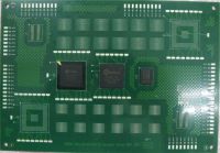
The test coupon for this study is shown in Figure 1. The dimensions of the coupon are 7.2” (183mm) by 5” (127mm) with the PCB thickness of 0.059” (1.5mm). It is a 10-layer board with immersion silver surface finishing. Three daisy-chain BGA components assembled in the test vehicle are A-CABGA288-0.8mm-19mm-DC-LF305 (J3), A-PBGA324-1.0MM-23MM-DC-LF-305 (J4), and SDRAM DDR2 512M-bit 667MHz 1.8V 84-FBGA (U3). All test boards were pre-conditioned through a worst case scenario of Pb-free assembly environment, comprising 3, 5, or 7 reflow cycles @260°C peak for 10 seconds.
Bend testing was performed with uniaxial test machine with series controller. The four point bend fixtures were made of hardened steel. Rubbing on the rounded bend rollers was mitigated by use of thin non-slip adhesive tape that prevented direct contact of the steel fixtures with the composite board. The bend test details are shown in Table 1. The bend test setup is shown in Figure 2.
The tests in this study were done at a rate of 5,000 microstrains per second in order to achieve pad craters. This fast rate resulted in tests less than 2 seconds long, so a set level of deflection was used rather than terminating the test once activity is detected. Initial measurements of the printed circuit board without components were done to determine the basic fracture level of the board. Board deflection was recorded by crosshead displacement and translated to load. Initial tests were correlated to strain level, but strain was not measured on every sample.
Figure 1: Test coupon.
Page 1 of 5
Share on:


Suggested Items
AIM Solder’s Dillon Zhu to Present on Ultraminiature Soldering at SMTA China East
04/22/2024 | AIMAIM Solder, a leading global manufacturer of solder assembly materials for the electronics industry, is pleased to announce that Dillon Zhu will present on the topic: Ultraminiature Soldering: Techniques, Technologies, and Standards at SMTA China East. This event is being held at the Shanghai World Expo Exhibition & Convention Center from April 24-25.
AIM to Highlight NC259FPA Ultrafine No Clean Solder Paste at SMTA Wisconsin Expo & Tech Forum
04/18/2024 | AIMAIM Solder, a leading global manufacturer of solder assembly materials for the electronics industry, is pleased to announce its participation in the upcoming SMTA Wisconsin Expo & Tech Forum taking place on May 7 at the Four Points by Sheraton | Milwaukee Airport, in Milwaukee, Wisconsin.
Hentec/RPS Publishes an Essential Guide to Selective Soldering Processing Tech Paper
04/17/2024 | Hentec Industries/RPS AutomationHentec Industries/RPS Automation, a leading manufacturer of selective soldering, lead tinning and solderability test equipment, announces that it has published a technical paper describing the critical process parameters that need to be optimized to ensure optimal results and guarantee the utmost in end-product quality.
Empowering Electronics Assembly: Introducing ALPHA Innolot MXE Alloy
04/16/2024 | MacDermid Alpha Electronics SolutionsIn the rapidly evolving electronics industry, where innovation drives progress, MacDermid Alpha Electronics Solutions is committed to setting a new standard. Today, we are pleased to introduce ALPHA Innolot MXE, a revolutionary alloy meticulously engineered to address the critical needs of enhanced reliability and performance in modern electronic assemblies.
New Book on Low-temperature Soldering Now Available
04/17/2024 | I-Connect007I-Connect007 is pleased to announce that The Printed Circuit Assembler’s Guide to… Low-temperature Soldering, Vol. 2, by subject matter experts at MacDermid Alpha Electronics Solutions, is now available for download.